INOX Group will set up a new quantum materials lab at the Indian Institute of Science (IISc) to support advanced semiconductor and quantum technology developments.
The plans were confirmed with a signed Memorandum of Understanding (MoU) between INOX and IISc. The lab will be based the IISc’s Centre for Nano Science and Engineering facility.
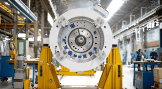
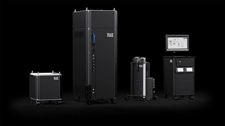
As part of the project, the duo will build an indigenous Molecular Beam Epitaxy (MBE) unit, a highly specialised piece of equipment for thin-film deposition.
With its efforts, the duo hope to prevent importing semiconductor and quantum computing technology at high costs. It also aims to to develop a strong workforce and will offer opportunities to undergraduates.
Siddharth Jain, Director of INOX Group, said, “Our contribution towards building the INOX Quantum Materials Lab at IISc Bangalore reflects our commitment to advancing scientific research and supporting India’s leadership in cutting-edge quantum technology, and allowing it to set new benchmarks and trends.”
Additionally, INOX and IISc have confirmed plans to conduct annual workshops on quantum technologies. It will also share research papers and encourage global conference participation.
Professor Srinivasan Raghavan, Chair of CeNSE at IISc, said the collaboration marks a significant step in making advanced technologies more affordable and accessible, while driving research in quantum technology and materials.
“The collaboration marks a significant step in making advanced technologies more affordable and accessible, while driving research in quantum technology and materials.
Quantum computing is still an emerging technology and is making significant strides in various sectors, including energy, providing insights for material development, supply chain optimisation, gas leak detection and environmental monitoring.
The role of specialty gases in semiconductor manufacturing
Specialty gases are often thought of as the lifeblood of the electronics industry and the beating heart of semiconductor manufacturing. These gases, including those used in creating silicon for chips, are directly linked to the advancement of current technology. Remarkably, a single wafer – a thin slice of semiconductor material crucial for integrated circuits – can comprise up to one thousand chips.
Semiconductor manufacture may use up to 30 different gases in all the various processes, including gases such as helium, nitrogen, and argon, which are used to create an inert atmosphere, flush chambers at the end of a process, or before cleaning.
Other specialty gases such as hydrogen, ammonia, and chlorine, in addition to less common examples like hexafluoroethane, octafluorocyclobutane and germane, are used in the etching and deposition processes.
MENA Industrial Gases Conference
In 2024, the Middle East & North Africa region home to both an enviable climate in renewable resources and investment and a bold vision in decarbonisation, green energy and industrial value chains.
From Saudi Arabia to Qatar, the UAE to Oman, and Mauritania to Morocco, there are promising gas and energy ecosystems-in-the-making. Vision 2030 is the mantra, and global leadership the goal.
But how can a vision for 2030 translate to a vision for industrial gas and equipment growth?
Join gasworld in November 2024 as its MENA Industrial Gases Conference 2024 returns to Abu Dhabi.
To attend, sponsor and for more information, visit: https://bit.ly/GWMENA-S24